

Since beginning this craze with nixie tubes and all things electronic, I have always wanted to fashion a watch from cold cathode displays. A nixie tube watch features timeless neon aesthetics combined with highly integrated semiconductors, placing it at the summit of geek jewelry.
Before I could lay the groundwork for my design, I needed to establish a few requirements for the scope of this project. Those details are as follows:
- 4 tube display
- Bluetooth 5.0
- Direct drive (as opposed to multiplexed)
- USB-C
- Ingress protected
- Glass and metal case – no plastics
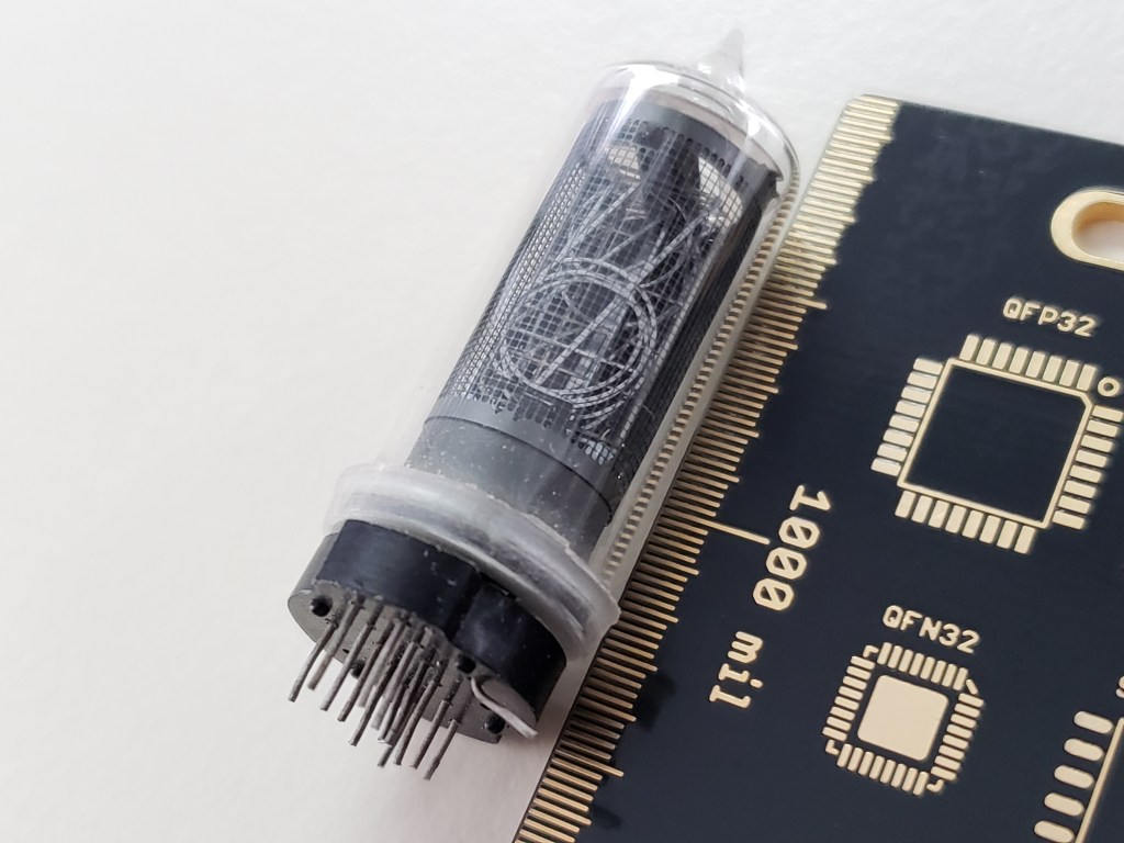
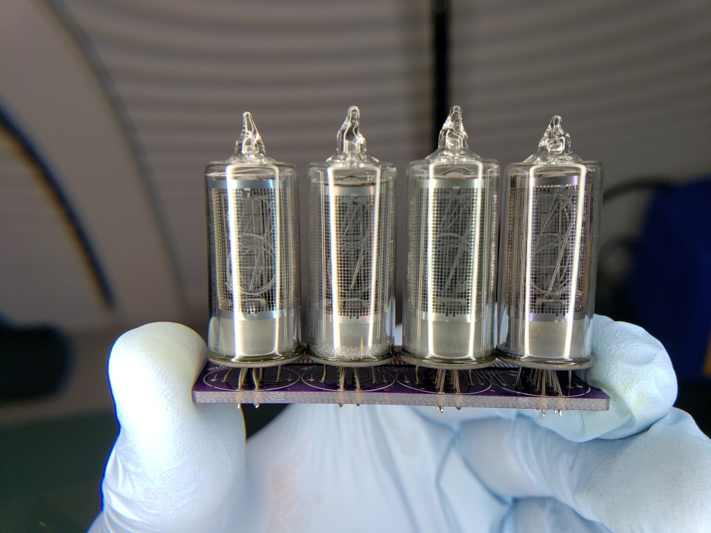
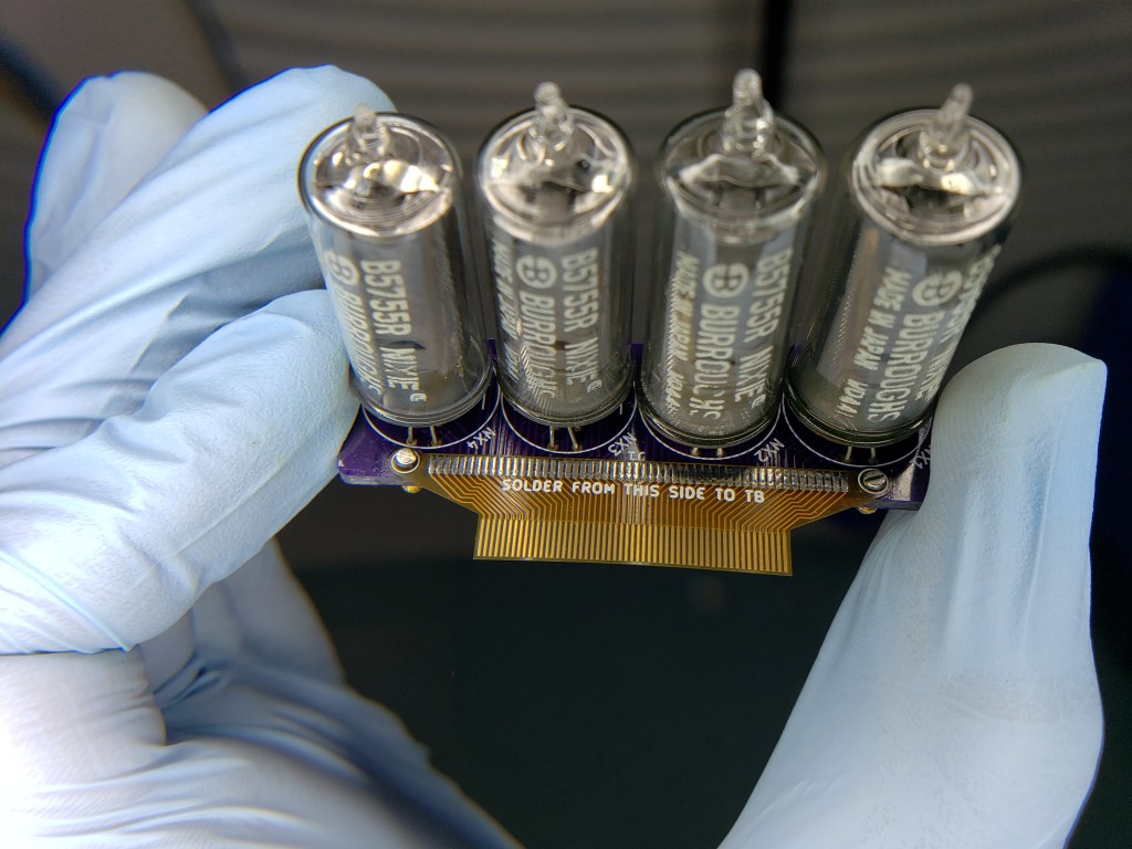
As this project has always been on my list, I had already scoped out and purchased the tubes I thought would be most appropriate. The Burroughs B5755R nixie was one of the smallest front facing tubes made, featuring a fine anode mesh and dual decimal points which will also be used to good effect.

I also found some scarce datasheets for similarly sized tubes, and a few application notes from Burroughs in the 1960’s which reference the 5755R nixie:
But before I could jump into the high density design that a 4 tube nixie tube watch would require, I wanted to practice my hand at a few working circuits. If you recall the portable geiger counter project, I took that schematic and shrunk it down as small as I could using prototype PCB services such as OshPark. Generally, you are limited to 6 mil trace/space, a max of 4 layers, and no blind/buried vias with low cost PCB prototyping services. Not truly HDI by today’s standards, but for a board that I have to hand assemble it was small enough.
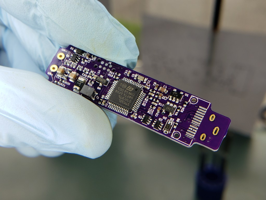
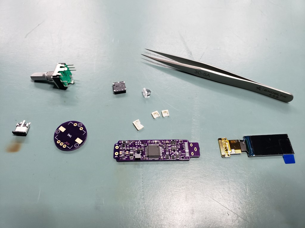
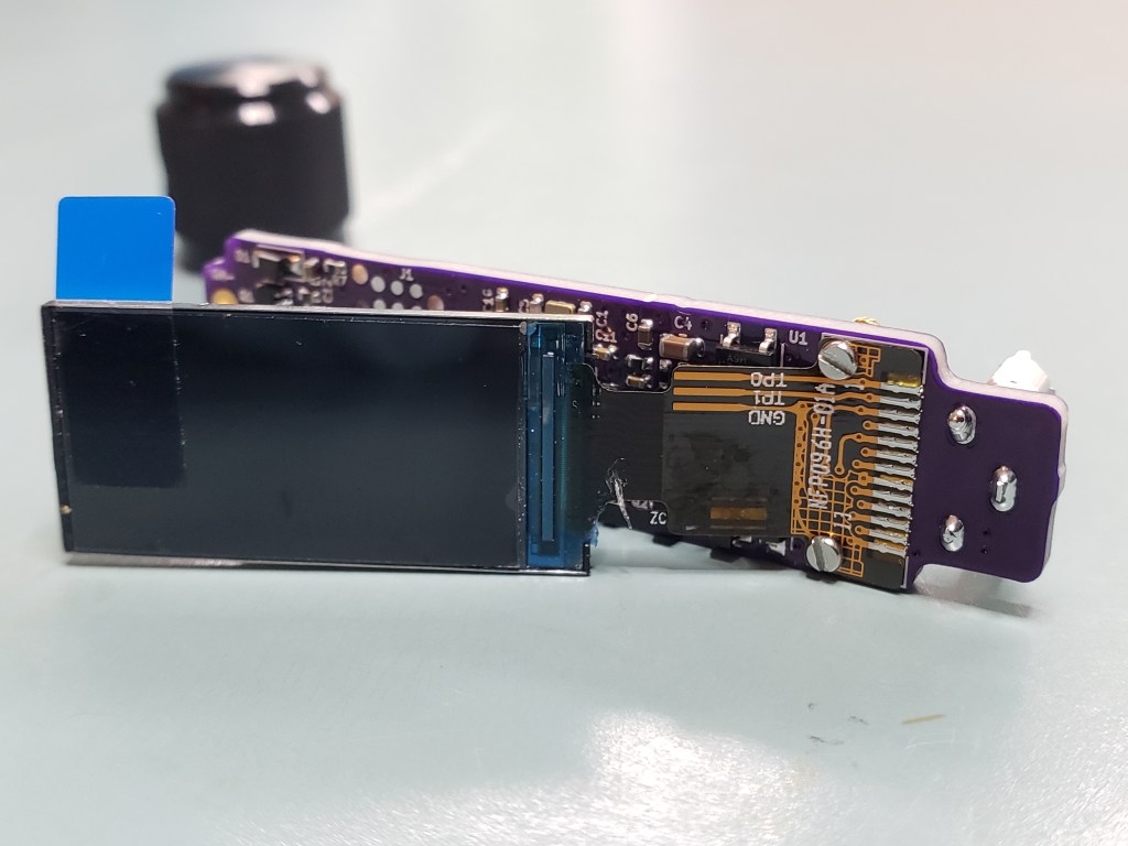
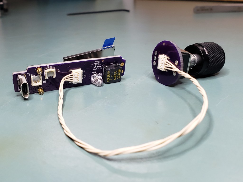
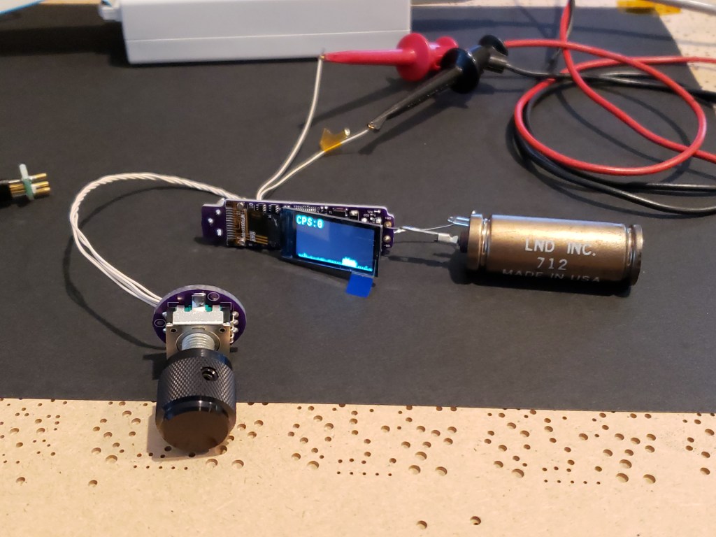
You truly have not experienced insanity until placing lots of 0402 components my hand. From start to finish, it took about 2 hours to go from a bare board to having all of the top side SMT components reflowed. A challenge, and a valuable learning experience.
Now that I am starting to become more comfortable with smaller and higher density designs, there was one other major hurdle I wanted to overcome before designing the first revision of the watch.
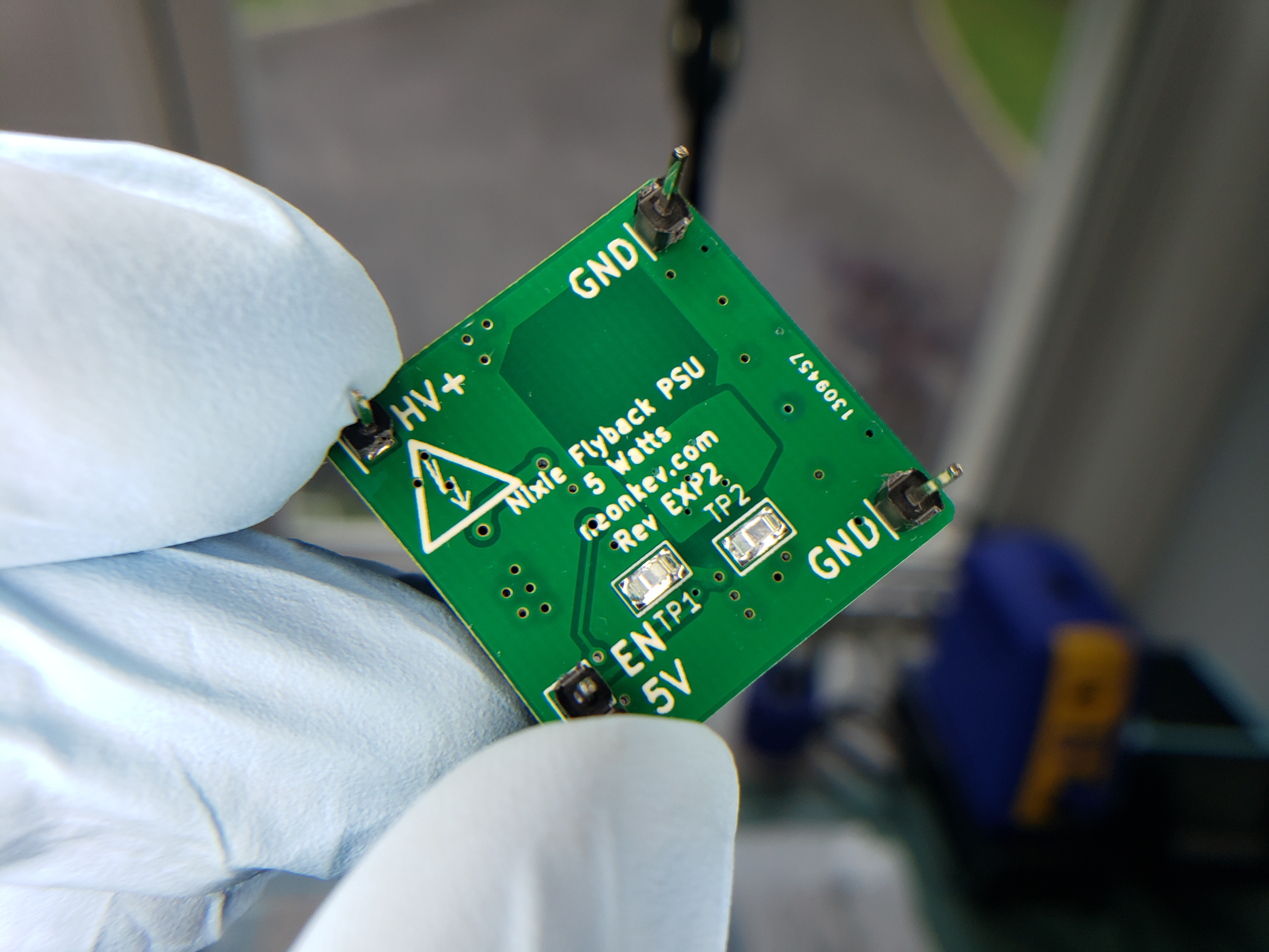
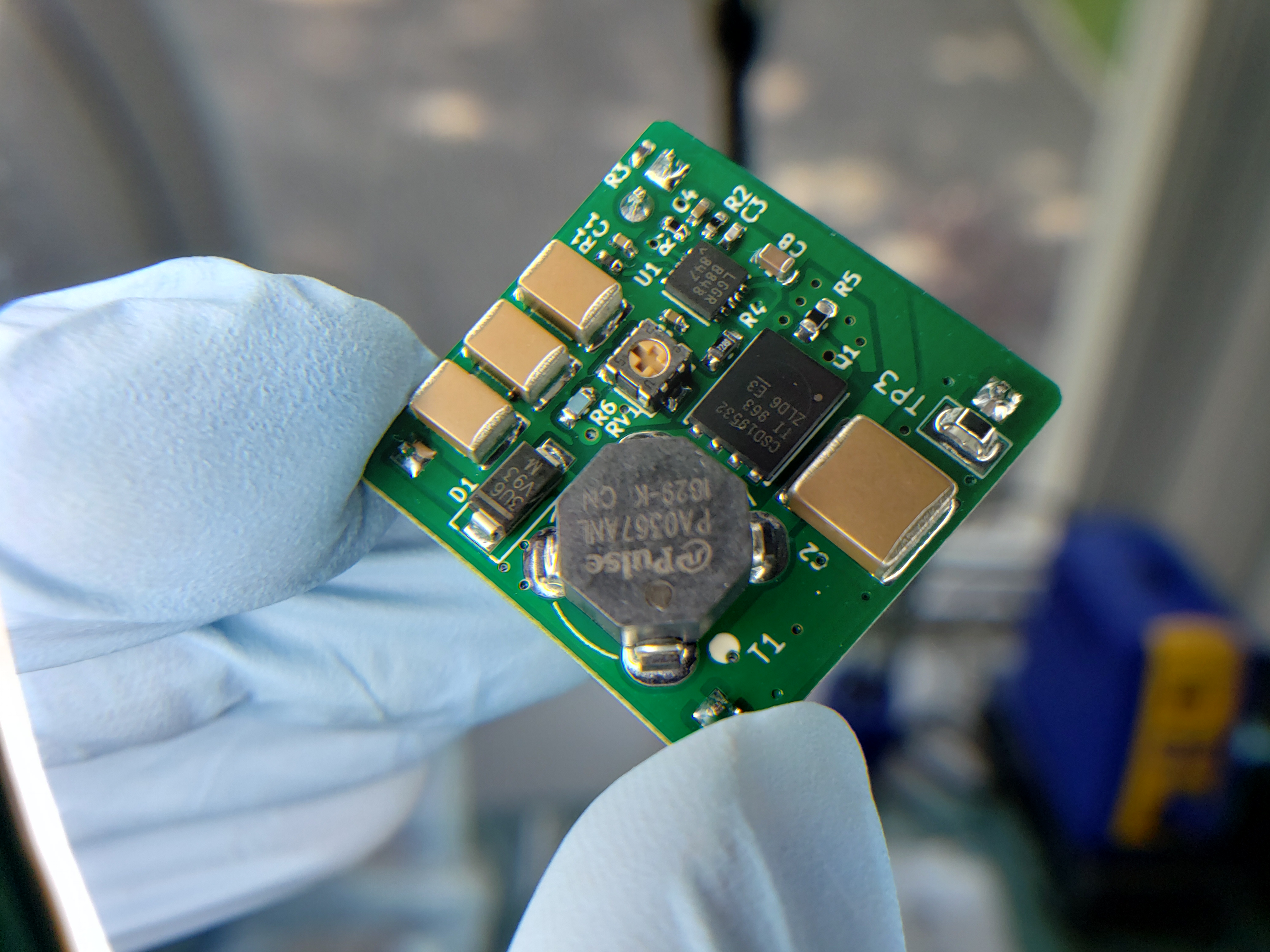
Generating a continuous high voltage output from a single cell lithium battery (180 volts from ~3.7 volts) is no mean feat, especially in a setting where both size and efficiency are extremely important. I anticipated the maximum current consumption of the (4) B5755R nixies to be around 10 milliamps at full brightness, which each tube on and displaying a digit. I set about designing an assortment of compact high voltage power supplies to evaluate for use in the watch:
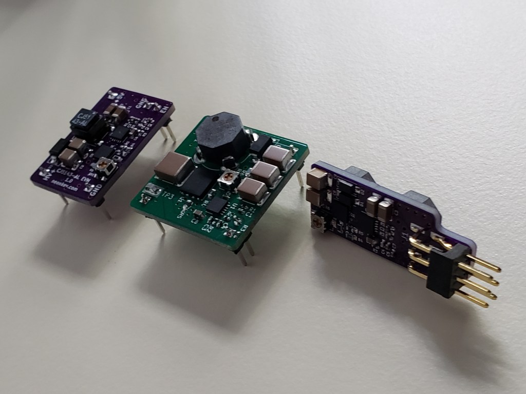
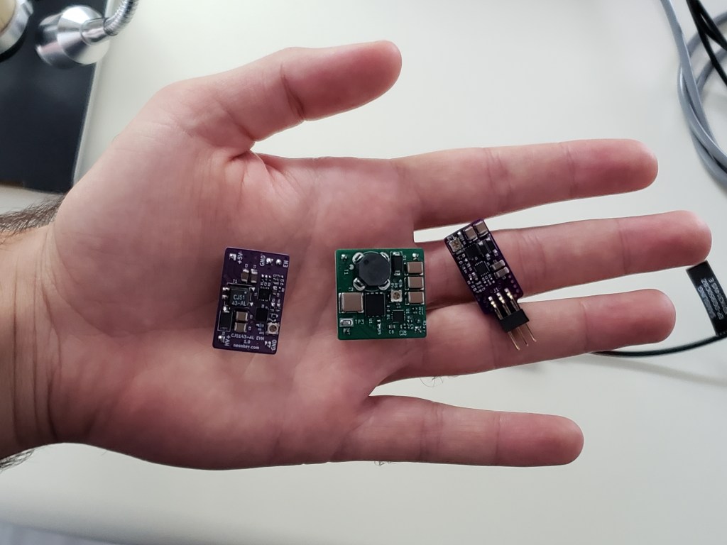
The circuits were based on the LT-3757AFE boost controller, which I found to be desirable based on the low external component count and current mode control scheme. I evaluated two different COTS flyback transformers which were among the smallest I could find with suitable specs: the Pulse PA0367A and Coilcraft CJ51-43AL. I’ve found that the transformer is indeed the trickiest single component to find a perfect fit for in a specialized switched mode power circuit; performance and size for a particular application often warrant a custom solution with high NRE costs. Since I wanted to stick with an off the shelf part I settled on the PA0367A with a switching frequency of 100 KHz. This combo gave me the greatest power capacity in addition to having a high average efficiency of 81%.


I was now poised to begin work on the watch itself. In order to get the bluetooth functionality I wanted, I originally had the NRF52840 in mind. This was, up until recently, Nordic Semiconductor’s flagship bluetooth low energy (BLE) system on chip (SoC). As badly as I wanted to use the 52840, the package options it comes in really are not compatable with rapid prototype PCB design rules. The 73-VFQFN package with dual ball rows is a real pain to work with; it really does require via-in-pad layout at the least, if not blind or buried vias which drive up the costs of your board exponentially. The other package choice was a chip scale BGA which is totally out of the question for a low cost prototype PCB.
To get around this and stick with my favorite board suppliers (namely OshPark), I downgraded my choice of processor to the NRF52832, which comes in the much friendlier VFQFN48 package. It is up there in performance with the 52840 (using the same Cortex M4F CPU) but doesn’t have quite as much memory, and also skimps out of a few other fancy peripherals. For my design, it will still be ideal for the brain of a smart watch running the latest BLE stacks.
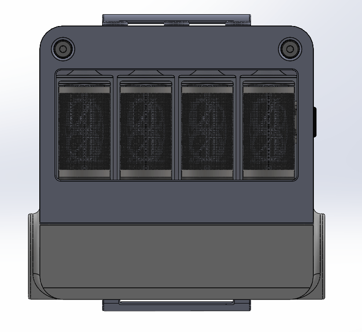
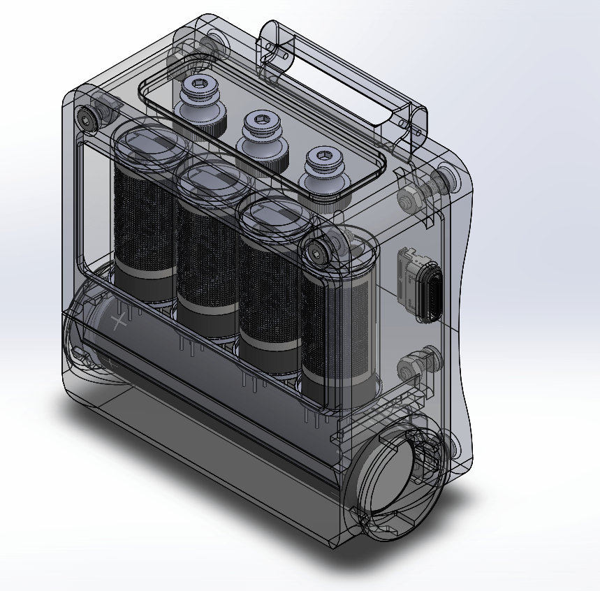
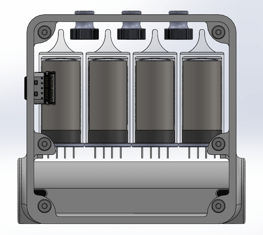
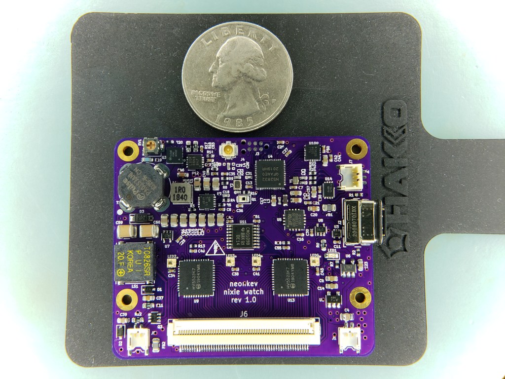
Before designing the boards, I first came up with the mechanical design. There is no point in doing a layout without having an established space claim. Knowing that the tallest component was going be the flyback transformer, I allotted enough distance between the planned board real-estate and the tubes, while trying to minimize the outer dimensions of the case. This is supposed to be a watch after all, and at 59mm square and 21mm deep, it will be quite hefty even with this level of optimization. My plan is to have the case and covers SLM printed from aluminum, which should allow for some intricate details that subtractive machining would not usually permit. The glass bezel and top window (where the capacitive touch buttons will be) will be custom cut from gorilla glass.
Now that I have an idea of how large my boards can be, it’s off to the races with a first revision schematic:
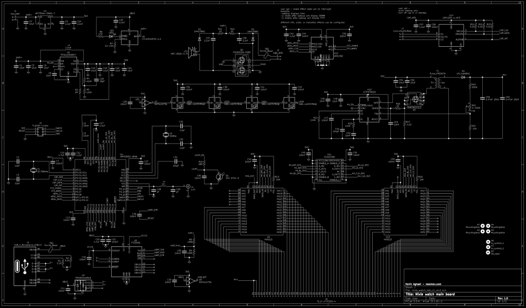
In addition to the NRF52832 and the high voltage circuit we already discussed, a few other design details of note are as follows:
- ADXL362 – mems accelerometer with ultra-low power wakeup mode
- CAP1293 – 3 channel programmable capacitive touch controller
- TPS61230 – synchronous 5V, 97% efficient boost controller for high voltage pre-regulation and other peripherals
- LT4054 monolithic battery charger
- (4) PWM addressable RGB LEDs for backlight
- Phototransistor light sensor for automatic nixie tube dimming
- Magnetic buzzer for audible communication
- Optional vibration motor
- UART for wired communication
- TVS input protection for USB connector
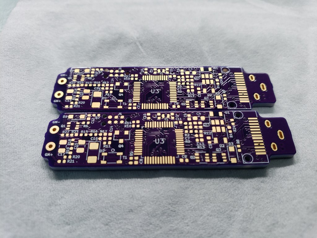
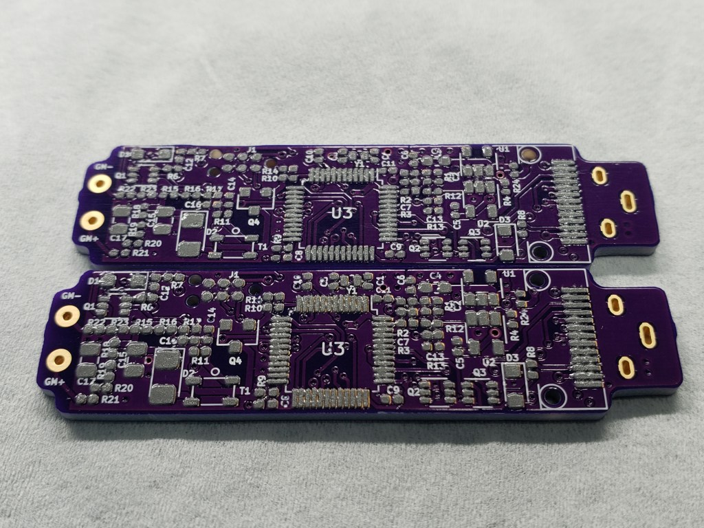
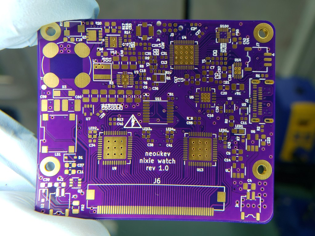
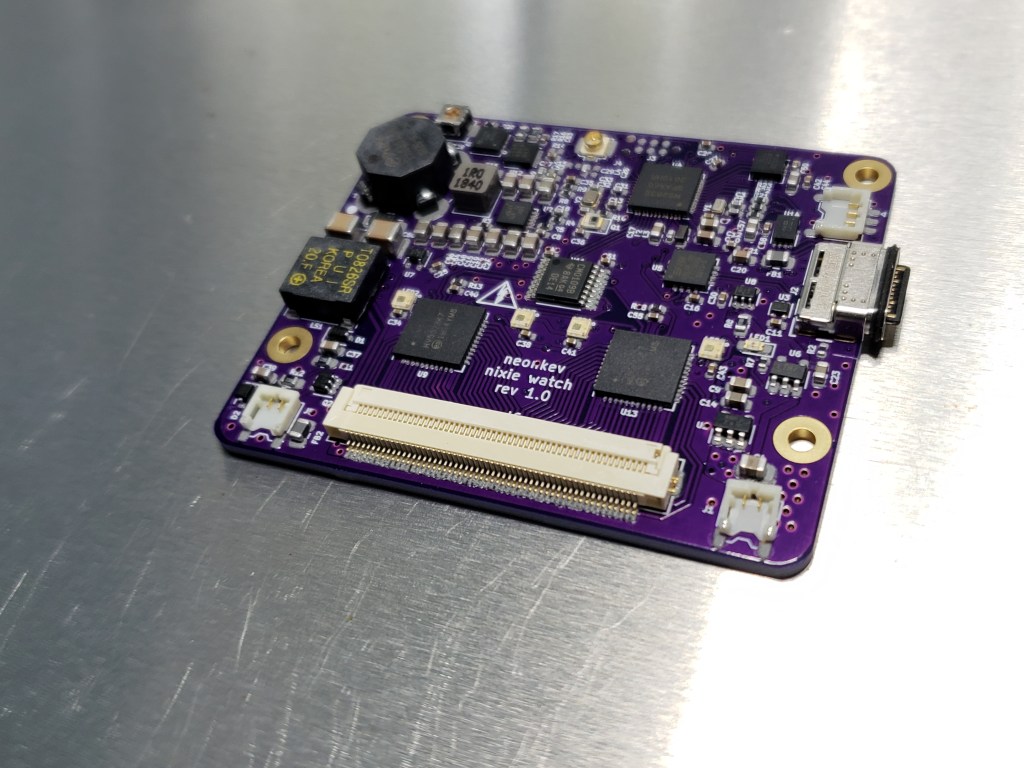
The Rev1 layout:
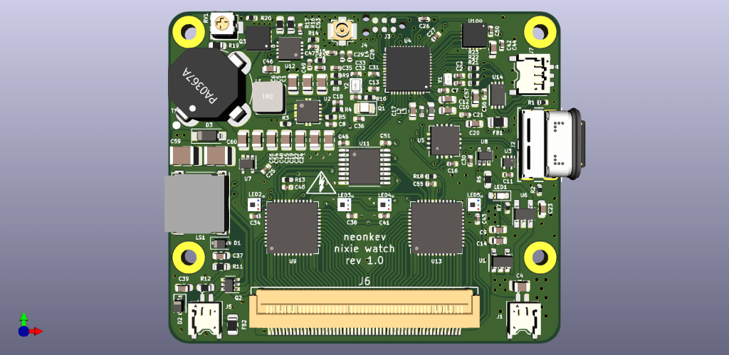
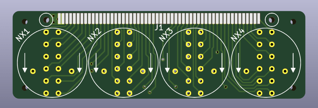
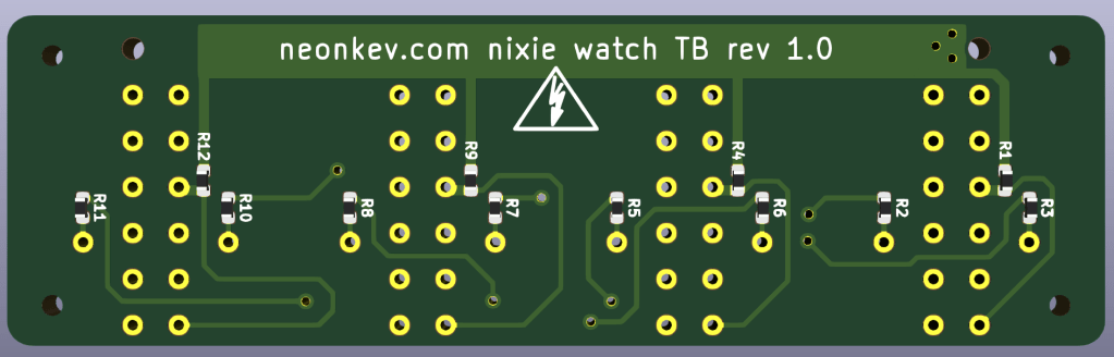
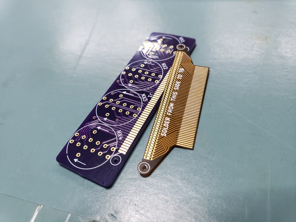
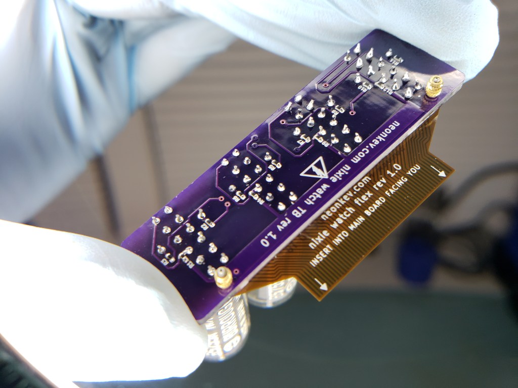
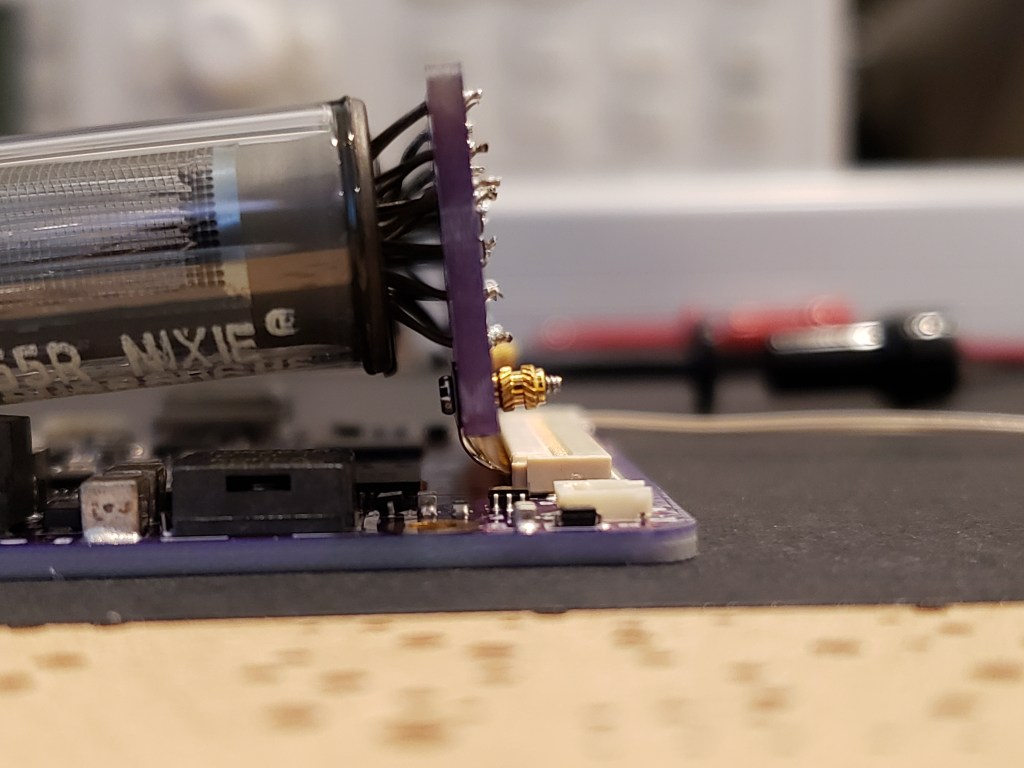
There are two boards in this design; one is the main board and the other is a tube board. In order to keep the main board design as universal as possible, I wanted the anode and cathode resistors for the nixies to be on the tube board. This way, the main board could theoretically be used as a stand alone nixie tube clock with any set of tubes. The connection from the tubes to the main board is accomplished across a large 54 position ZIF connector – necessary since each cathode (10 numerals + 2 decimal points per tube) are being driven directly with the HV5523 high voltage serial to parallel open drain ICs.
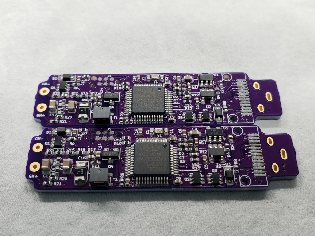
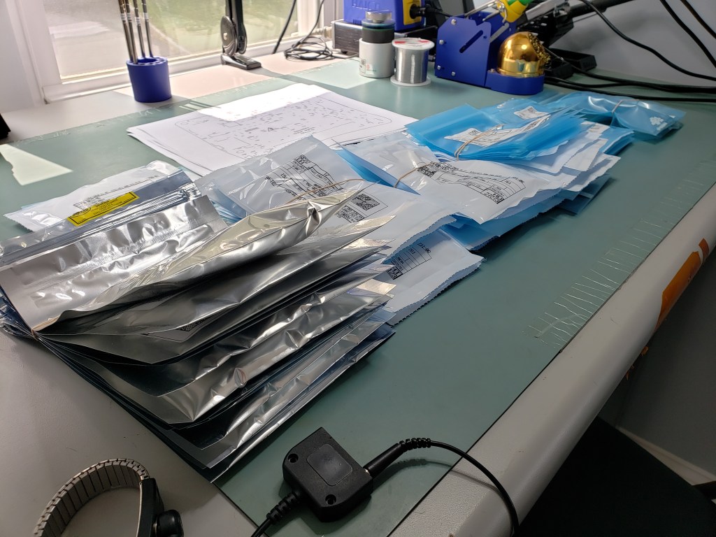
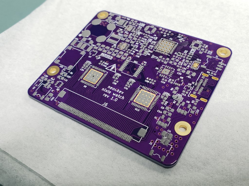
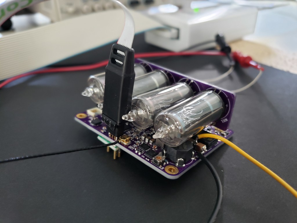
After weeks of waiting, the boards and parts finally arrived! Ensue hours of painstaking hand assembly:

Now its only a matter of time before I’m able to get it programmed! I have zero experience with the NRF52 ecosystem, but I have been able to communicate with the board using serial wire debug (SWD) and flash several examples to the 52832. The plan is to develop in VSCode using platformIO and Zephyr RTOS framework. Looks like I’m going to be learning a lot about device trees if I want to get this board up and running.
More updates to come; stay tuned!

That is a great article. The furthest I ever got with a ‘portable’ nixie clock was to design a power supply. Though I have added LiPo batteries to multiple clocks, I wouldn’t call any of them particularly compact! As you say, finding a good off-the-shelf transformer is not easy. The specs on that one (1.5A saturation current, 1:12 turns ratio, 180mΩ primary resistance) are very good. It would be nice if sites like digikey allowed you to search on those parameters.
I used a LPR6235-253LMRB in a one-tube clock and a Wurth 749196141 in a four tube clock. I will have to give the PA0367A a try.
LikeLike
Wow that’s really cool!
LikeLike