
Added 10/22/19: 40 watt converter now available on Tindie! https://www.tindie.com/products/18278/
Since beginning work on the highest power nixie power supply anyone would need, I made several discoveries which were instrumental to getting my inductor based converter working. If you are following along from my previous post regarding the first revision of the 40 watt design, you might remember that I concluded with the idea that I needed a larger inductor. This turned out to be only one of several changes needed to achieve the desired input-output levels I was aiming for. Naturally, my first attempt at the problem was to make an educated guess. Just change the inductor and see what happens.


Turns out neither of these was an improvement; in fact, they reduced performance by dropping out at higher input voltages. This, however, led me to an important conclusion: I needed a higher saturation current inductor.After having tried a total of four (4) different individual inductors at different switching frequencies, the best result (lowest dropout input voltage) came from the 1mH 3.5 amp inductor I originally began testing with!Because I could not find a single inductor solution, I ended up paralleling two (2) of the 1mH 3.5 amp inductors. Doing so halves the inductance but doubles the current. Other benefits from this arrangement are lower parallel resistance and improved heat dissipation.

At last, I was closing in on 12 volts at rated power! I got down to 12.5 volts and the controller cut out again. Now, the challenge had become personal. I came too far to give up at 12.5. There has to be something I’m missing!At the point where a sane person would call it quits, I began combing through the TPS40211 datasheet for any hints which could point me in the right direction. I read each page word-for-word.Knowing that this is a current mode controller, I figured that something about the current sense control loop was becoming unstable at these low input voltages. I had already experimented with changing the shunt resistor; I found that lower values had improved dropout performance marginally, but not enough to make or break my goal. Section 7.3.8 of the TPS40211 datasheet “Current Sense and Sub-Harmonic Instability” describes a phenomenon which I had previously thought extraneous, but now realized was the key to my success. All current mode boost controllers are prone to a condition known as sub-harmonic instability when operating at 50% or higher duty cycle. As described in Unitrode (now owned by TI) application note U-97:
“Gain peaking by the inner current loop can be one of the most significant problems associated with current-mode controllers. This peaking occurs at one-half the switching frequency, and – because of excess phase shift in the modulator – can cause the voltage feedback loop to break into oscillation at one-half the switching frequency. This instability, sometimes called sub-harmonic oscillation, is easily detected as duty cycle asymmetry between consecutive drive pulses in the power stage.”
That is not very encouraging. However, the TPS40211 datasheet goes on to describe a solution for sub-harmonic oscillation:
“The remedy for this condition is to apply a compensating ramp from the oscillator to the signal going to the pulse width modulator. In the TPS40210/11 the oscillator ramp is applied in a fixed amount to the pulse width modulator. The slope of the ramp is given in Equation 17 (pictured):”

Then, the note that sparked an idea:
“It is possible to increase the voltage compensation ramp slope by connecting the VDD pin to the output voltage of the converter instead of the input voltage as shown in Figure 26. This can help in situations where the converter design calls for a large ripple current value in relation to the desired output current limit setting.”
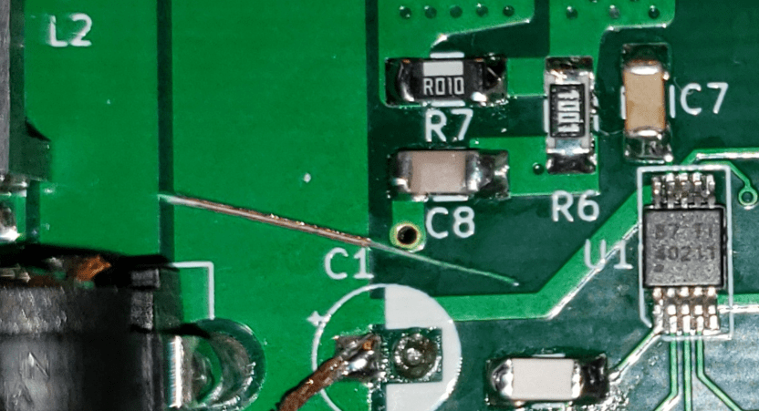
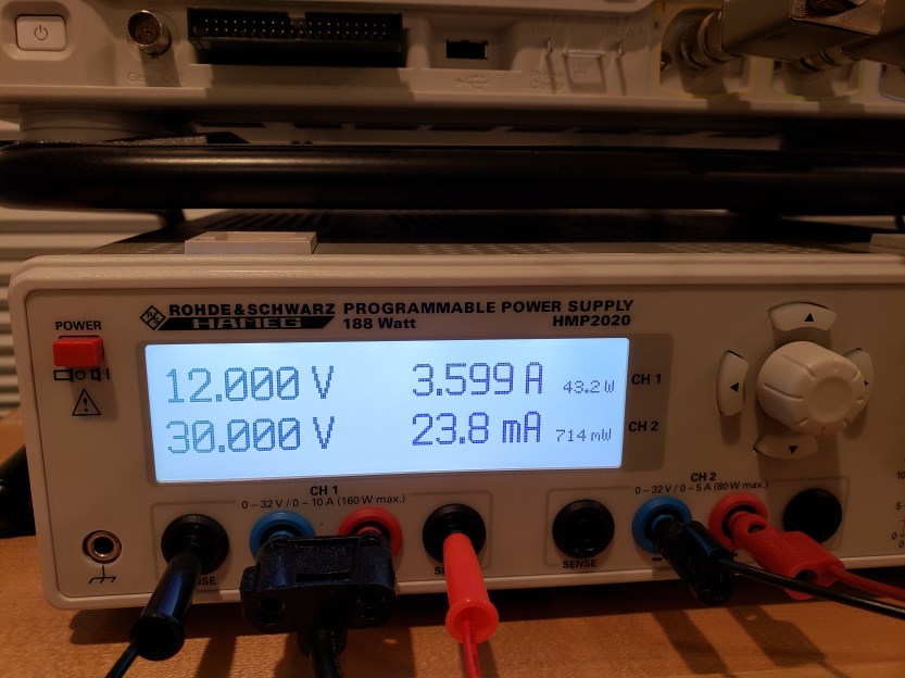
Clearly, my converter “calls for a large ripple current value in relation to the desired output current limit setting”. At a 15:1 boost ratio, I need to switch well over 3 amps of low voltage to get 0.2 amps of high voltage out.I decided to try running the logic at a different, higher voltage than the power section. If you recall from equation 17, the slope of the compensation ramp of the TPS40211 is a function of switching frequency and logic voltage (VDD). I already tuned my switching frequency to get the most out of my inductors, so the only variable left to change was VDD itself. I cut the trace going to the controller IC, and hooked it up to channel 2 on my power supply.
Since the TPS40211 is rated to operate between 4.5 to 52 volts, I thought 30 was a good place to start. Channel 1 set to 12 volts, channel 2 set to 30 volts.Well what do you know; it works!
Finally! Mission accomplished. Now, all that remained was to design these changes into the new revision.


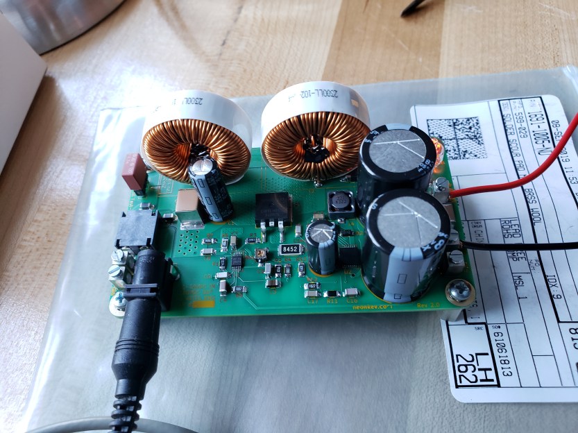
Behold! Revision 2 includes a small, integral, wide input DC-DC converter for providing the TPS40211 controller with the voltage it needs to operate with stability at low power input voltages. Additional improvements include:
- Improved PCBs
- High TG FR4 (170)
- ENIG finish
- 2oz copper
- Rigorous board quality control
- High ripple current, long life electrolytic capacitors (Panasonic and Rubycon)
- SiC (silicon carbide) automotive grade Schottky diode
- C0G/NP0 ceramic capacitors for signal, X7R for decoupling
- Input side wire-to-board terminal blocks
- Socketed, replaceable 6.3 amp fuse
- Trim pot for high voltage (continuously adjustable from 170 to 190 volts).
- Mixed cap input (added ceramics for improved transient and frequency response).
- TVS (transient voltage suppression) diode for input surge protection
Amazingly, revision 2 worked on first power up! With the TPS40211 being powered at a higher voltage than the input, and with the improved layout and higher spec components, the supply pushed 200 milliamps out all the way down to 8.4 volts in!
After running for 3 hours, input settled at 12.0 volts, 3.31 amps for an output of 179.0 volts, 202.3 milliamps (91% efficiency).
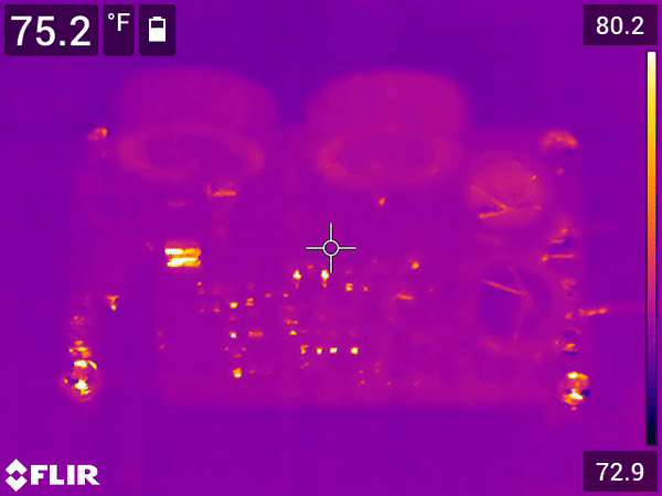
Some thermal images of power up, steady state operation, and cool down (in that order). Temperatures were quite low, with the hottest component being the feedback resistor at around 55-57°C peak.
Of course, the thermographist inside me cannot resist:
This is certainly has not been a cheap board to make; the BOM (bill of materials) in low quantities (< 10) on Digikey is approximately $77 USD for a single board! Add in the cost of the PCBs at $10 a board, and materials for assembly (forget about labor, research, and development)… I don’t see this being a profitable enterprise. However, I am planning a release on Tindie to cater to the small market of neon enthusiasts who can make use of an overbuilt high voltage power supply. Stay tuned!

Nice build!!!
LikeLiked by 1 person
This is very nice work…
LikeLike