
DC-DC voltage regulators are essential in nearly all modern electronic goods.
Most electronics have one fixed input voltage, and many individual voltage regulators to locally power circuit components. Semiconductor devices such as common integrated circuits, processors, memory might all require different operating voltages. It is simply not practical to feed these different voltages in from multiple power supplies. Instead, one, maybe two common voltages are distributed on rails or PCB planes, and if a different voltage is needed in one section, a DC-DC regulator is used to attain the final required voltage for that component.
DC-DC regulators exist is many sizes and topologies. The two major types are Linear regulators and Switching regulators.
Linear regulators can be very simple, consisting of only a resistor and a Zener diode.

Image courtesy of Wikipedia user BatManFascination
In this arrangement, a higher voltage (Vin) is applied across the diode. Once the “zener voltage” is reached (which is much lower than a conventional diode), the zener diode conducts to ground. A series resistor is added to prevent the zener from passing to much current and blowing up.
More complicated arrangements of linear regulator exist. For example, a MOSFET may be used in place of the zener as the semiconductor element. A negative feedback loop with an error amplifier may be added to drive the transistor gate for precise and fast output voltage regulation. Higher performance linear regulators may also feature low drop-out (LDO), which means that for a given output voltage the input can be a lower voltage (typically a few hundred milli-volts above input) than for a non-LDO linear regulator (typically 1.5 – 2.5 volts dropout from input).

Image courtesy of Linear Technologies application note 140 – October 2013
Still, the fundamental operating principal of any linear regulator is the same: the input voltage is higher than the output, and the difference is merely being turned into heat. Linear regulators offer low output noise, no EMI to surrounding devices, and are usually cheap, but are electrically inefficient in addition to not being able to boost output voltage over the input. You might already be thinking that this arrangement it isn’t suitable for high voltage/high power applications. You’d be right.
Enter the switching regulator. Utilizing the magic of magnets, switching regulators can step the output voltage down (buck) or up (boost) at high power levels, and with efficiencies upward of 90%. How is this possible?
A switching regulator, as the name implies, switches the input DC at frequencies generally between tens or hundreds of kHz to leverage the effects of magnetism. When the main switching transistor is turned on (usually a MOSFET), power flows from the input into an inductor. The core of the inductor is then magnetized, meaning magnetic flux is present and the inductor is now storing energy in the form of a magnetic field. The amount of energy stored is described by:

Where ‘E’ is energy in joules, ‘L’ is inductance, and ‘I’ is the peak current through the inductor in amps. (This is probably derived from Maxwell’s equations and proving it is well beyond my mathematical faculties. Feel free to comment if you have the proof).
Then, before magnetic saturation is reached (the point at which the inductor core reaches its highest flux capacity), the MOSFET is switched off. The magnetic field in the inductor collapses, producing energy though the same coil that originally magnetized it.
Now, the energy discharged from the inductor must be routed to the output “smoothing” capacitor(s). This is done usually in one of two ways; with a diode, or with a second transistor. With a diode, this type of switching converter topology is known as an “non-synchronous” converter. When a transistor is used instead, this is referred to as a “synchronous” converter.

Image courtesy of Brian King – Texas Instruments
Non-synchronous buck/boost regulators are smaller, less expensive, and less complex than synchronous designs, but also operate at lower efficiencies mainly due to voltage drop across the “catch” diode.
Synchronous regulators are more efficient thanks to the lower voltage drop of the extra MOSFET, but are more complicated to design and are overall more expensive.
Congratulations. You now know the basic operating principals of DC-DC switching regulators. In practice, however, there are a lot of tricks that an experienced power electronics engineer will use to optimize a design for a specific application; whether it’s high efficiency, low footprint, high power… you name it. The real skill is in the component selection and physical layout of the entire circuit.
Minimizing the ESR of your output capacitors to lower output ripple, inductor core materials and core losses, good PCB layout to minimize noise from power switching elements into signal circuits for the controller IC, thermal management… the list goes on. It is a topic too broad to cover in a single blog post, and I am by no means a veteran power electronics engineer. The literature is plentiful for an in-depth analysis of each and every aspect of switching converter design, because it really is a topic that extends to every facet of modern electronics.
Now that you’re all warmed up on the topic, let me introduce one of my projects: a 20 watt, 12 volt to 180 volt boost converter.
This is a high voltage power supply I wanted to put together for nixie related projects. It is based on the Texas Instruments TPS40211 boost controller. The circuit in mind is designed to deliver a solid 100 milliamps at 180VDC from a 12 volt input; plenty considering most individual nixies usually use between 2-5 milliamps per tube. Board dimensions are 3.32″ x 2.19″ (84.45mm x 2.19mm). The TI switching controller features an enable/disable control which can be pulled to logic high (1.2~10V) to shut the switching circuit down, say, with an external micro-controller.
My first revision, before I did any reading on switching converter layout, was a complete and utter failure. I didn’t bother populating any boards of this design.

How NOT to design a switching regulator. Look at those skinny traces going to the inductor and the MOSFET (T1… yeah, ” T “)… what was I thinking?!
After I realized that my first layout was a complete abomination (including the reference designator for the transistor), I moved forward with Revision 2.

WAY better. Notice the large copper power planes on the input and output, the short gate drive trace from U1 to Q1, as well as a separation of the power electronics from the controller and signal quadrant. There were a few errors I touched up as well (if you can spot them).
After ordering my Revision 2 boards from JLCPCB on a Wednesday, they arrived promptly from China the next Monday. Time to populate them!


To my surprise, the circuit worked! When I first powered it up, nothing happened (like I expected). Turns out the MOSFET gate drive pin wasn’t connected to the pad on the board. Once I reworked that small mistake, the circuit came to life! A solid 180 VDC was now present on the output. Time to stick some resistors across this baby and put my creation to the test!
The results:
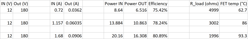
75-80% efficiency from low to high load, respectively. Now bad at all, considering where I started and the fact that all this learning and designing was done in about a week.
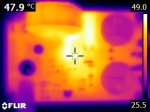
A look at the thermal performance:

First issue I noticed is that the output voltage feedback resistor (R5 – 51K) is getting hot. Makes sense… 51K across 180V will dissipate almost 2/3 of a watt. The component I used is 1 watt rated… but this is still not ok. The application notes for the TPS 40211 suggest using a feedback resistor betweek 10-100K. I started in the middle but it seems we need to go towards the higher end of that scale. Going above 100K might reduce noise sensitivity to an undesirable degree, so I’ll make this resistor 90K. Also, adding a “heatsink” by stitching one side of the resistor to a copper pour on the other side of the board should better dissipate the now halved heat.
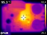
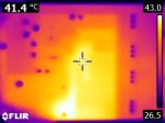
Now to monitor heat from the power electronics under load:


This is not surprising as well. Considering I implemented no thermal management for the transistor, it did generate and retain a considerable amount of heat. The max rated operating temperature is 150°C (~302°F), but I still want to manage the heat as best as possible through good board design. In addition to the feedback resistor changes, another major added feature will be heavy via stitching to heatsink the MOSFET to a major pour in the bottom of the board. In order to make room for this, I will also be transitioning from a surface mount inductor to a vertically standing through hole version.
The gained board realestate also permitted me to add an input protection fuse, in addition to an EMI filter on the low voltage side. It is a parallel damped filter I designed using TI’s online Webench utility. This filter should attenuate high frequency noise to keep it from entering and leaving the supply.
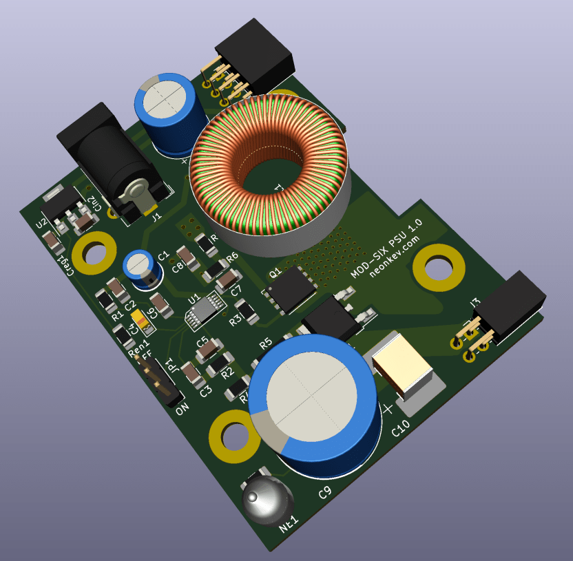
The Rev 3 layout is as follows:

Other added details include wire-to-board terminal blocks for the high voltage output, and a neon bulb to indicate whether or not high voltage is present across the output.
As of writing this, Revision 3 boards are ordered and being made, with 2oz copper thickness instead of 1oz as on the Revision 2 board. My goal is not to build the cheapest boost converter, but one that uses high quality components, has more grunt than I’ll ever need, and is engineered to the best of my abilities. Updates are soon to follow!
UPDATE: 8/29/2019
Revision 3 was assembled and tested successfully!

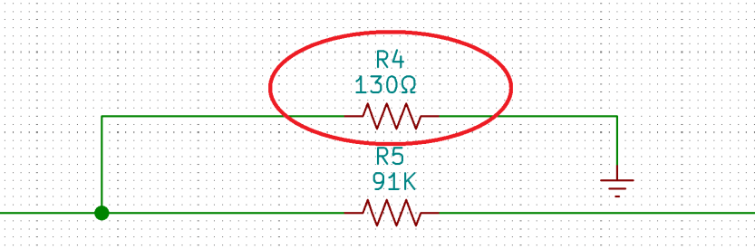
I made a few mistakes before I got it working though. First, in changing the feedback resistor to 91K, I forgot to change the other resistor in the divider!
Immediately when turning it on, the voltage shot past 180 all the way to about 320 volts!
After some pondering over what my mistake was, I realized that the feedback voltage was almost half of what it should be for the TPS40211. The voltage from 180 volts across the 91K and (erroneous) 73.2Ω divider is about 145mV, whereas the reference for the TPS40211 should be 260mV. The transistor let out some magic smoke before I could shut down the input supply. Whoops!
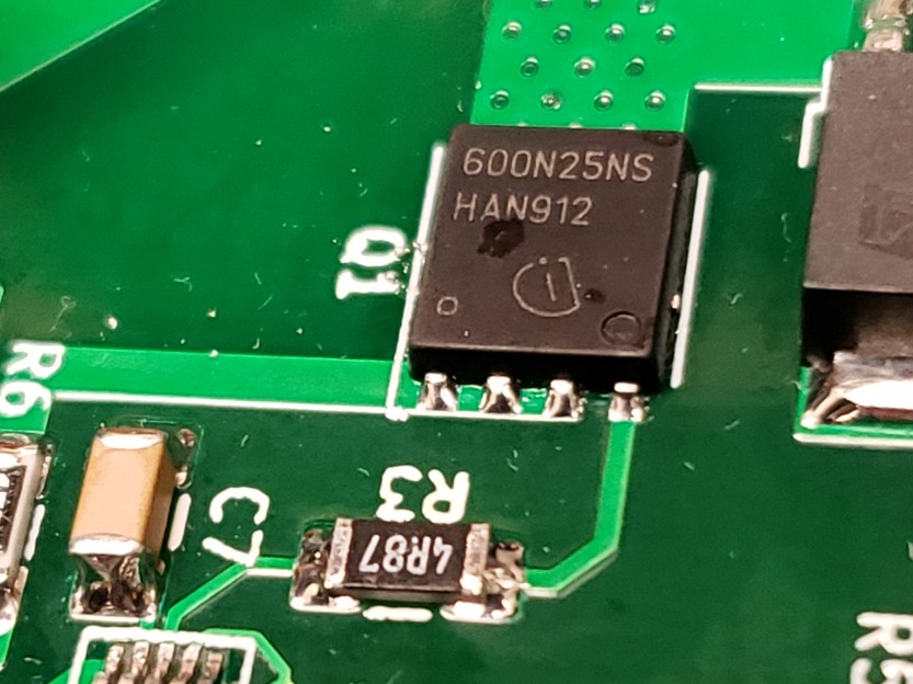
After replacing the transistor and R4 with the appropriate 130Ω resistor, my supply came alive. I also changed the soft start capacitor, C4, from 4.7uF to 10uF. I noticed that the supply would go into over-current “hiccup” mode when started with a higher ( >50ma) load.
Another change that should be made is to the shunt resistor, R7. Since the TPS40211 is a current mode controller, it detects current via the bias across this component. I again observed that above 90ma, the controller would go into over-current protection. Since I did not have a bunch of 1206 resistors in the 20-25 mΩ range laying around, I did my endurance testing at 85ma.


At 85ma load, the output ripple was about 4 volts peak-to-peak. I can live with 2.2% output ripple. Nobody is directly powering logic at 180 volts.
Efficiency and thermal performance also were improved from revision 2, largely due to the halved heat dissipation through the feedback resistor and via stitching around the MOSFET to heatsink Q1 on both sides of the board.

This has been an extremely educational experience. Switch mode power supplies offer a number of developmental challenges in terms of design. Efficiency, layout, heat dissipation, noise, stability… careful considerations must be made for each aspect of the design to strike an optimal balance between critical operating parameters.
Moving forward with my new knowledge, I’m planning a 10 watt version for use in the famous MOD-SIX nixie clock! Stay tuned.

It looks pretty beefy. These PS designs get non trivial really fast it seems!
LikeLike
Thanks! It’s definitely in the high power range for nixie voltages. I wouldn’t want to touch the output accidentally!
LikeLike