
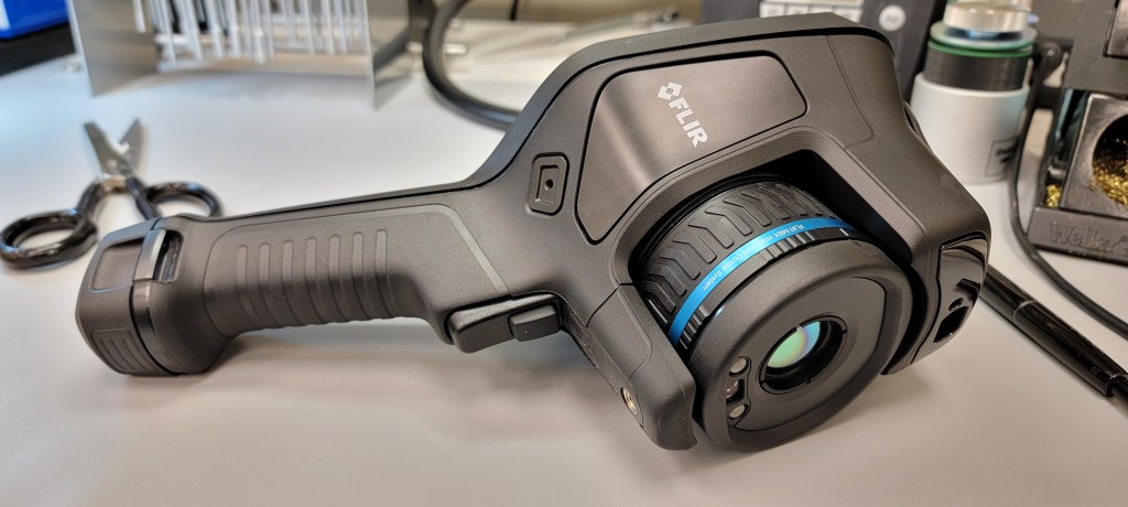
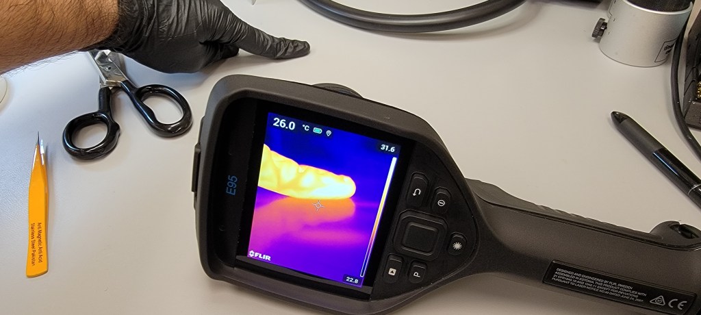
FLIR introduced the E95 in 2017 as the flagship product in their handheld E series lineup.
While it has been discontinued today and replaced by the upgraded E96, it is still a very respectable handheld thermal imager with relatively high resolution (464 × 348) at 30 Hz image frequency.
I would call the E95 a “midrange” camera as far as the handheld thermal imager market goes. Today, the highest spec. handheld offering from FLIR (on the commercial market) is the T1020 with an impressive 1024 × 768 thermal resolution at the same 30 Hz. It will set you back around $60K USD however, while a used, working E95 can be had around 4-5K on eBay.
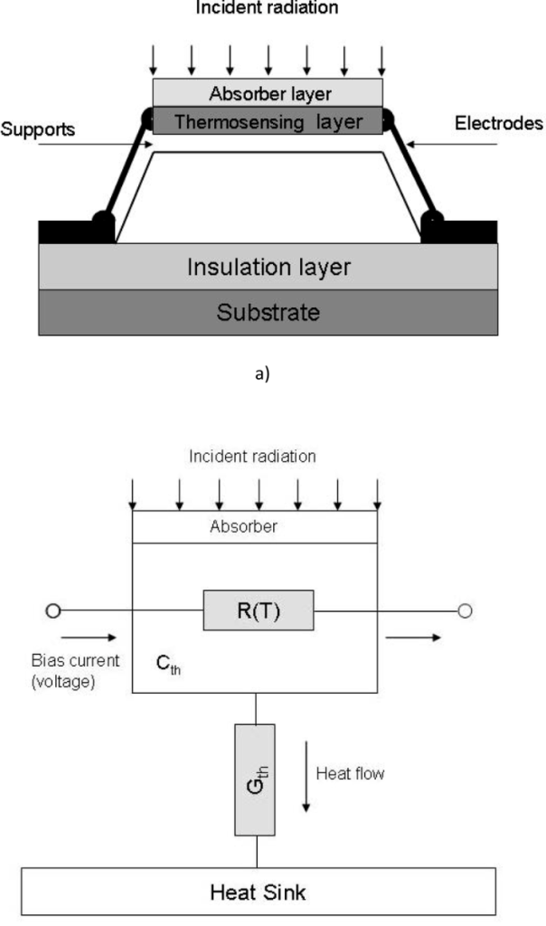
All of these handheld thermal cameras use an uncooled image sensor called a microbolometer.
A “bolometer” is a device which changes electrical resistance in response to radiant (infrared) head. A “microbolometer” is a type of sensor which has many bolometric pixels in a small area. Because most microbolometers are passive detectors, this means they are advantageous in terms of power consumption, size, reliability, and ease of use.
Thin Film Un cooled Micro-bolometers Based on Plasma Deposited Materials – A. Kosarev et. al, DOI: 10.1139/cjp-2013-0567
In comparison, there are thermal imaging cameras which employ active sensors (similar in design to common digital camera sensors for visible light, but using different semiconductor processes for infrared detection). These sensors require cooling due to the power dissipation of the semiconductor material used. Typical operating temperatures are cryogenic, between (-210°F to -170°F).
As you can imagine, the materials and machinery needed to operate cryogenic coolers are not suitable for a highly portable camera. While cooled cameras are more expensive and less portable, they offer superior performance in terms of image frequency, resolution, and sensitivity.
With that bit of context out of the way, lets return to our E95 teardown.
I have been using this camera for several years at work, and it recently developed an issue with the autofocus button. There are two triggers on the E95 grip; one is to activate the autofocus, and the other is to take a picture. With the autofocus not working, it makes operating the camera two-handed (to turn the focus ring) which is not great when doing electronics troubleshooting.
Because the autofocus would still activate when set to use the built-in laser range finder continuously, I believed that the problem is probably with the microswitch in the trigger itself. This would require disassembling and some troubleshooting.
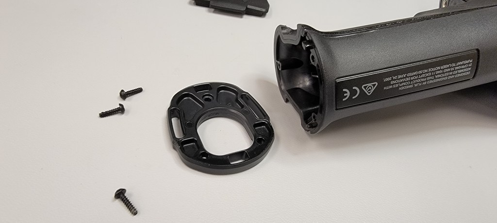
With no manuals or prior experience taking one apart, I first had to locate all the screws hidden under stickers…
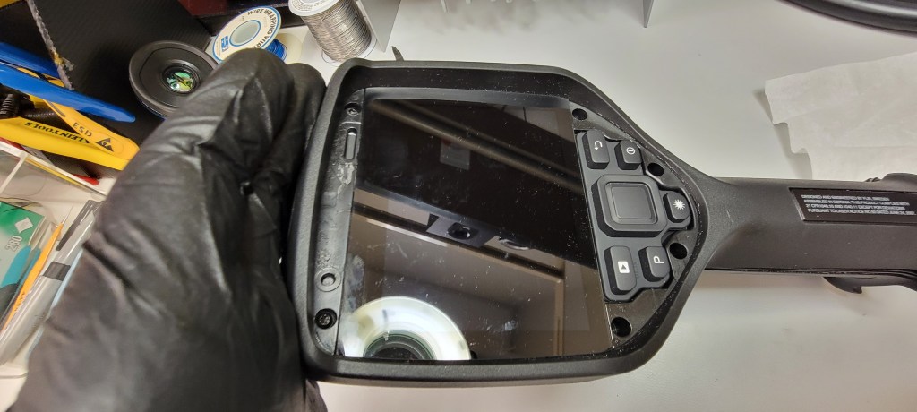
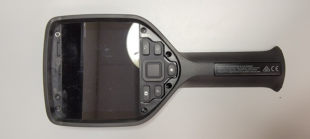
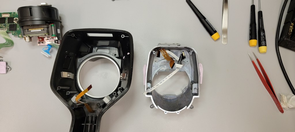
Now we can separate rear half of the camera (with the LCD, buttons, and speaker) from the main body. Carefully, of course, not to damage any of the cables/connectors. And there are quite a few of them.
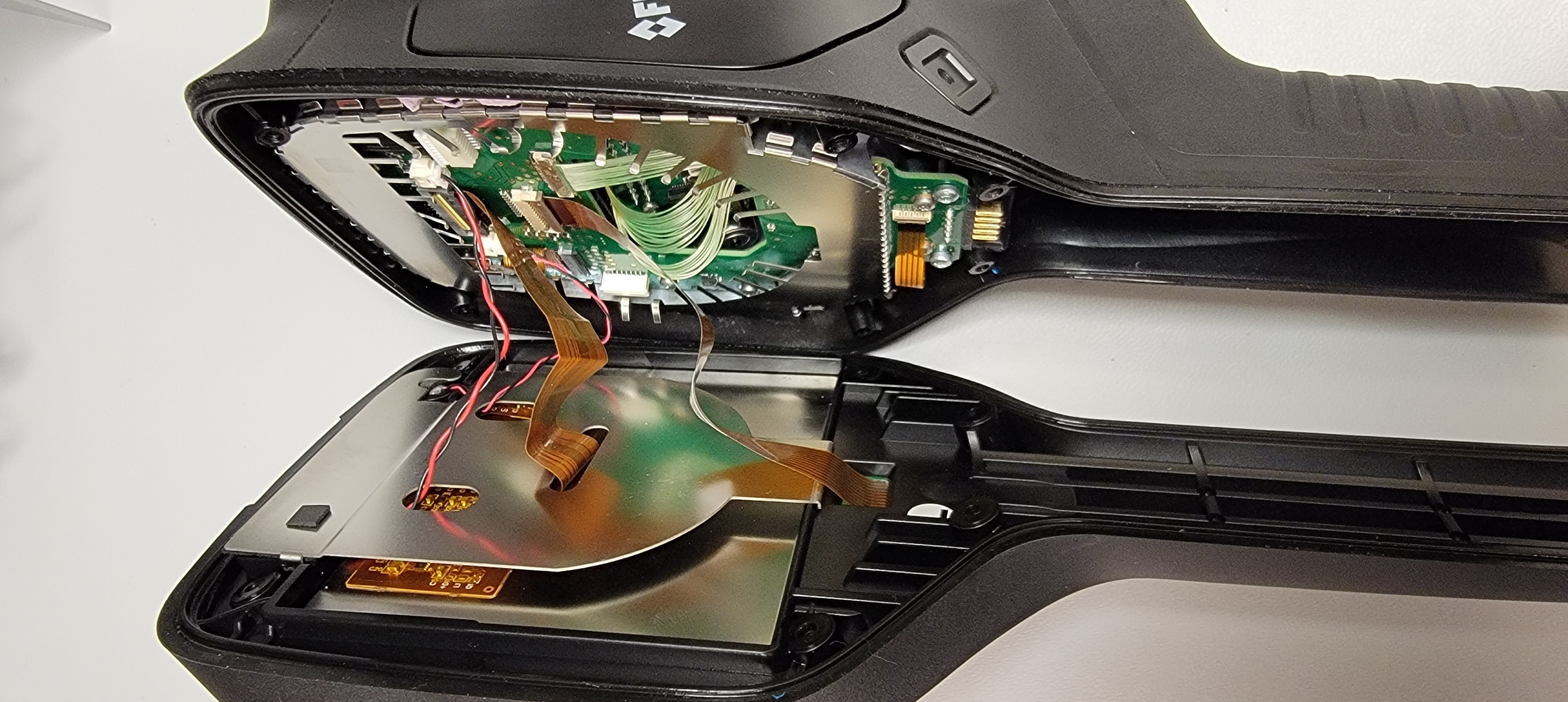
Setting the back half aside, now we can take a look at the main camera guts:
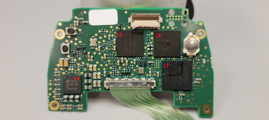
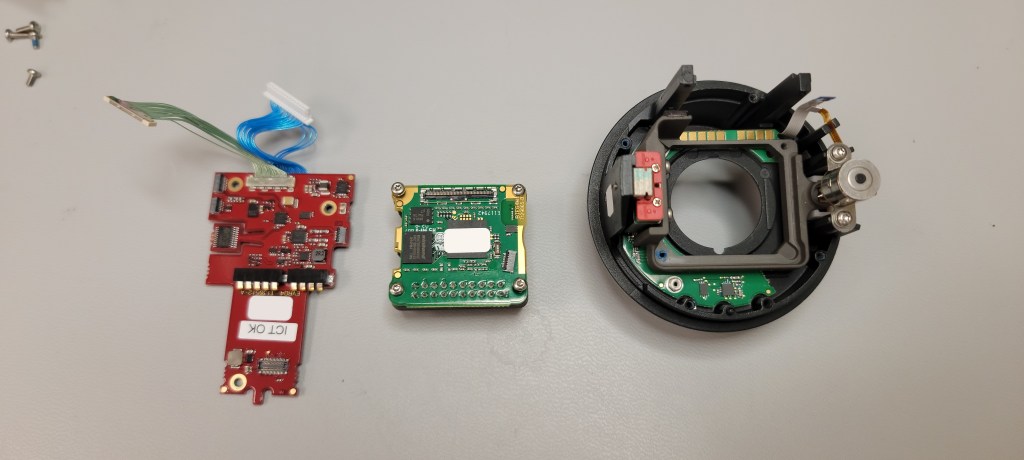
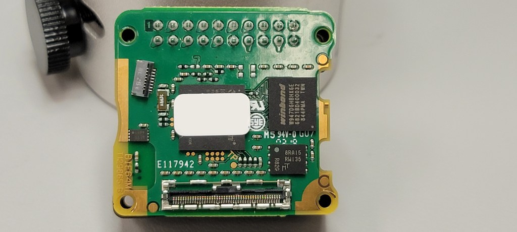
After popping out some shielding, we can remove the first PCB. This board appears to be mainly an interface backplane for power and signals between all the smaller subassemblies.
Taking a closer look at the board we just removed:
Some of the ICs noted with red numbers:
- 1 – TI AIC3100, Low-Power Audio Codec With Audio Processing and Mono Class-D Amplifier
- 2 – NXP PCA9534, 8-bit I2C-bus and SMBus low power I/O port with interrupt
- 3 – (same as 2), NXP PCA9534
- 4 – TI BQ24298, I2C Controlled 3A Single Cell USB Charger
- 5 – (same as 2 and 3), NXP PCA9534
- 6 – TI HD3SS460, 4 x 6 Channels USB Type-C™ Alternate Mode MUX
- 7 – NXP MMA8452Q, 3-axis, 12-bit/8-bit digital accelerometer
- 8 – Analog Devices ADT7420, ±0.25°C Accurate, 16-Bit Digital I2C Temperature Sensor
Moving onto the next bits:
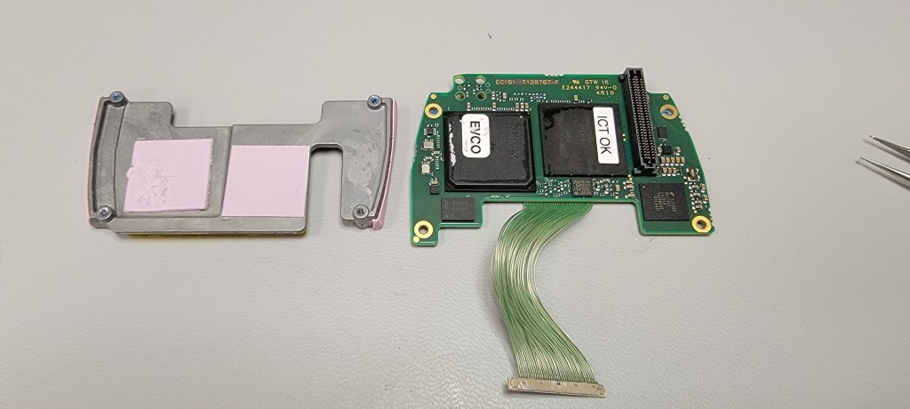
The next board appears to be the main processor and image DSP. Removing the heatsink bolted to this one:
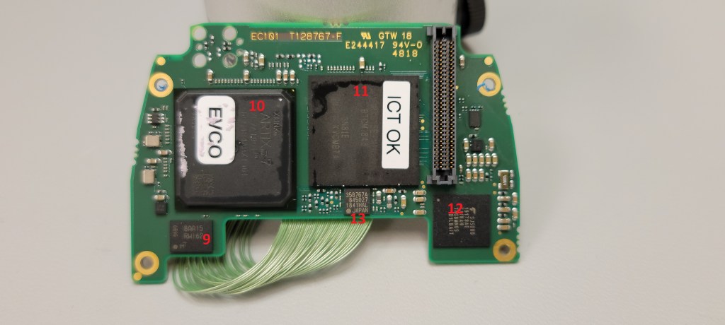
More IC analysis:
- 9 – Micron MT25QL256ABA8E12, FLASH 256MBIT SPI
- 10 – Xilinx Artix-7 XC7A100T-1CSG324I FPGA
- 11 – NXP MCIMX6S5EVM10AC, ARM® Cortex®-A9 Microprocessor IC i.MX6S 1 Core, 32-Bit 1.0GHz
- 12 – Kioxia THGBMNG5D1LBAIL, FLASH – NAND Memory IC 32Gbit eMMC 200 MHz
- 13 – Toshiba TC358767AXBG, bridge device that enables video streaming from a host (application or baseband processor) over MIPI DSI or DPI link to drive DisplayPort display panels
- 14 – Renesas/Dialog DA9063, PMIC 14.2A System (6 bucks + 11 LDO)
- 15 – Nanya NT6CL128, LPDDR3 4Gb SDRAM
- 16 – (same as 16), Nanya NT6CL128
- 17 – Altera Cyclone V 5CEFA2F23I7N FPGA
This little board does most of the heavy digital lifting. It contains a significant amount of FLASH and RAM, while also housing the main application processor and the gruntier FPGAs in the system, likely for processing raw or near raw outputs from the microbolometer. It also contains the video bridge/display controller to drive the LCD.
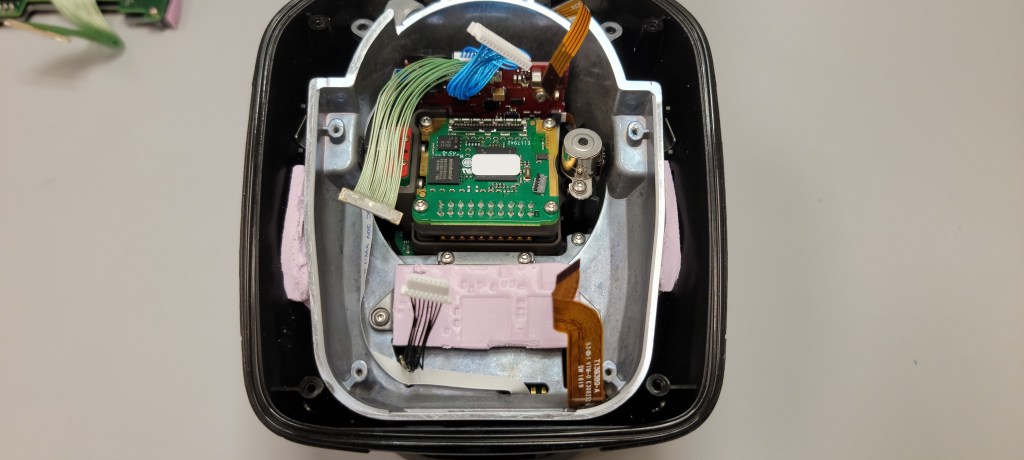
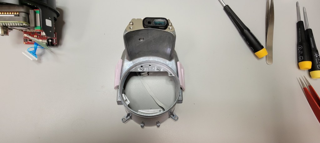
With those two PCBs out of the way, we need to remove the sensor/lens mount assembly before being able to drop the aluminum body out of the way.
This device is fanless, so the aluminum shell conducts most of the heat and dissipates it to the outside on the metal “cheeks” of the camera. Interesting thermal design but it works. Those cheeks get quite hot after the camera has been on for a while!
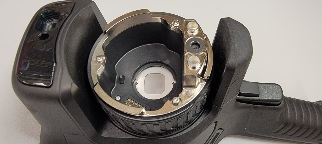
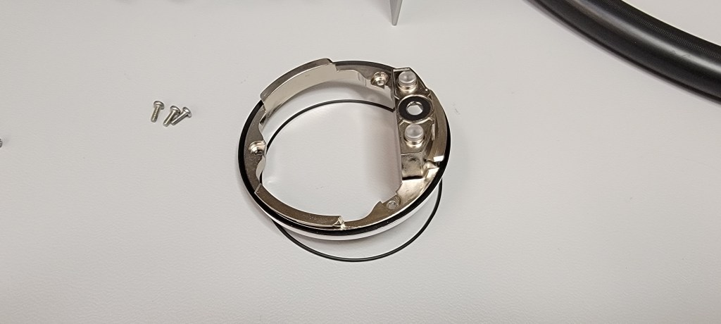
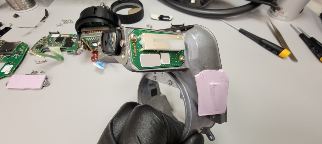
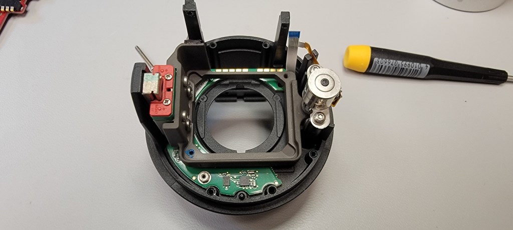
Once we remove the lens mounting ring, there are several screws from the inside that hold the entire sensor/focus assembly in place.
With this dropped out, we can continue to remove the aluminum shell. There are 2 more screws hidden near the top of the camera, behind the cover plate over the laser range finder assembly.
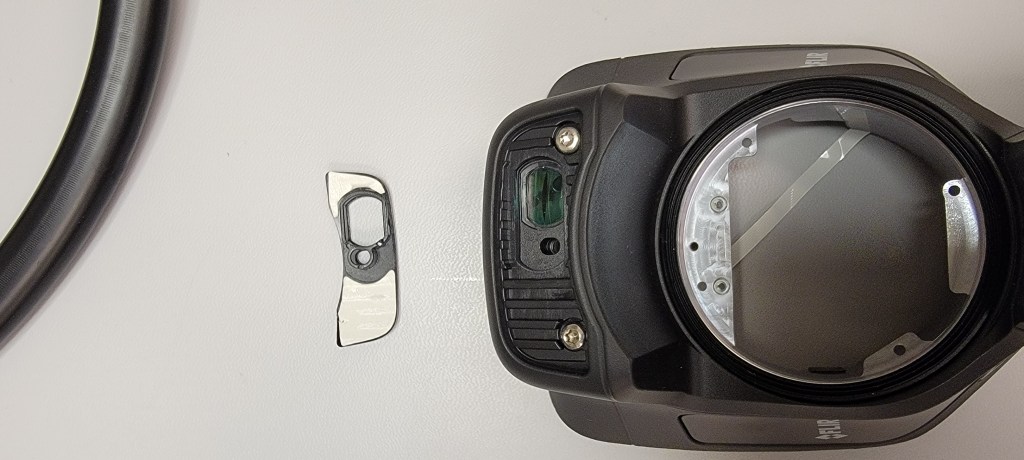
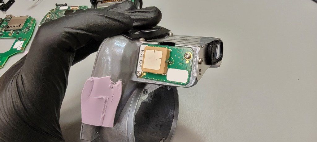
Now we can look at the small PCBs still bolted to the aluminum housing. These include the WiFi module, GPS module, and laser range finder.
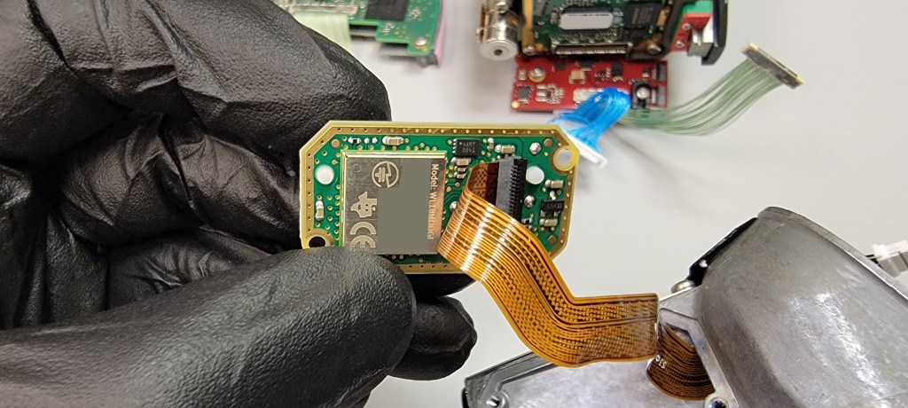
The WiFi module of choice is a TI WL1801MOD series combo module. This is actually capable of WiFi, Bluetooth, and Bluetooth low energy all in a single module.
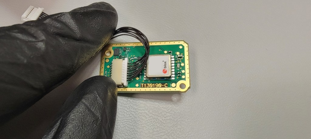
The GPS module is a ublox MAX-M8Q-0.
The laser range finder has a bit more going on. I’m not sure if this embedded module is a FLIR design or if they bought it as an off-the-shelf solution.
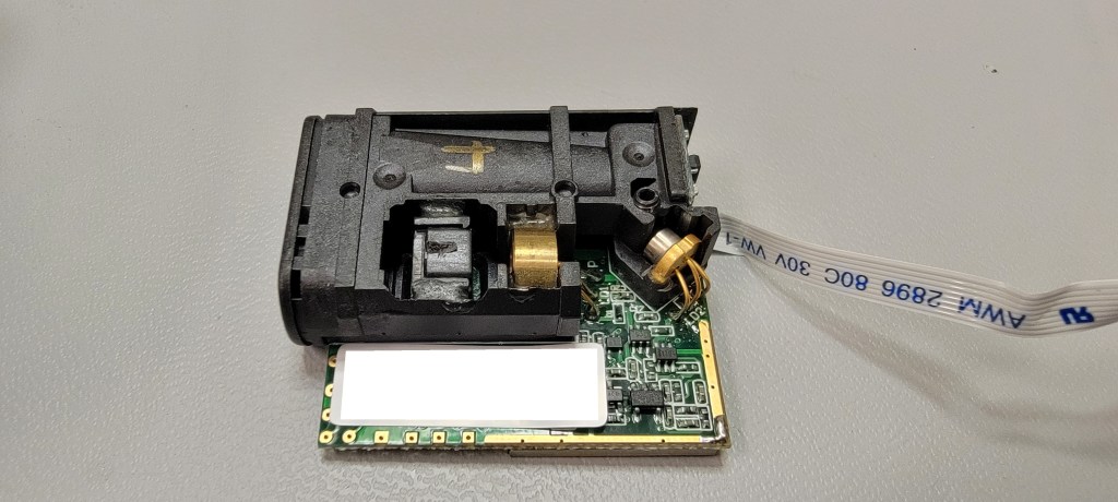
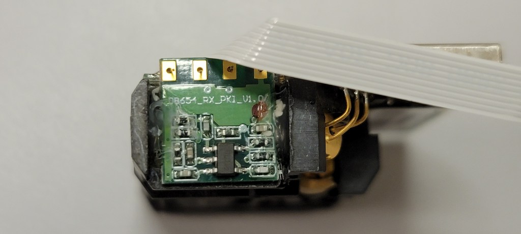
Taking a peel under the can on the laser range finder:
The 10-MSOP IC here is an Si5351A, I2C controlled clock generator. It uses a 25 MHz reference (the crystal next to it also is marked for 25 MHz) and internal PLL to generate frequencies between 2.5 kHz to 200 MHz. The 10-MSOP package has 3 clock outputs.
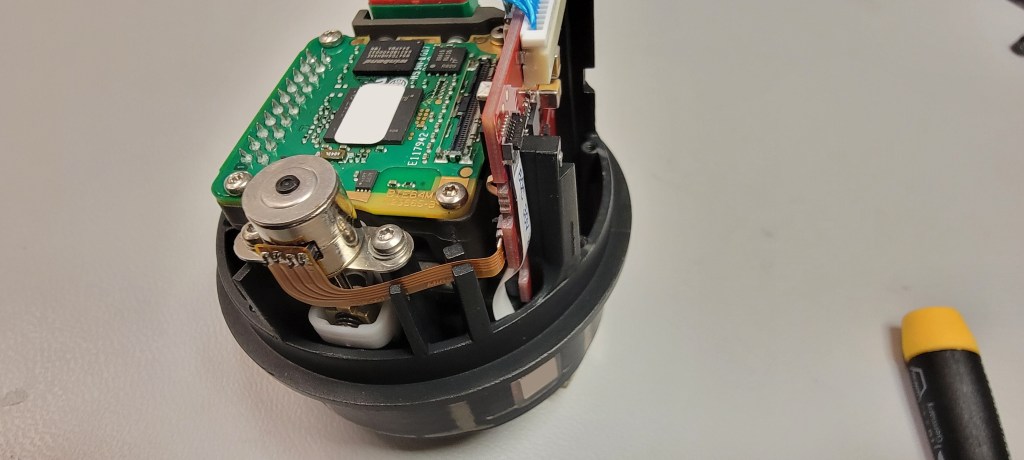
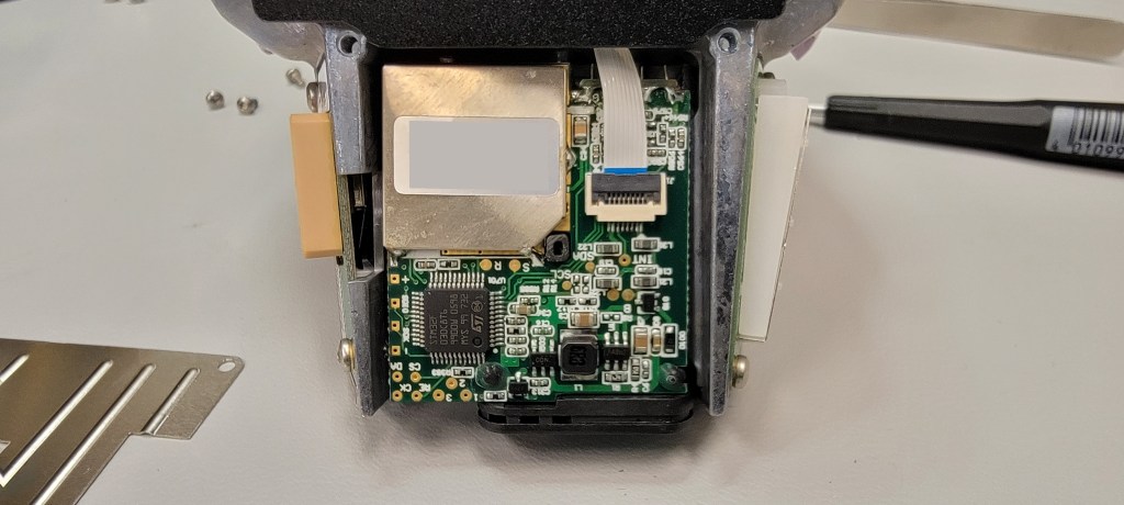
Continuing our teardown, let’s take a look at the heart of the camera:
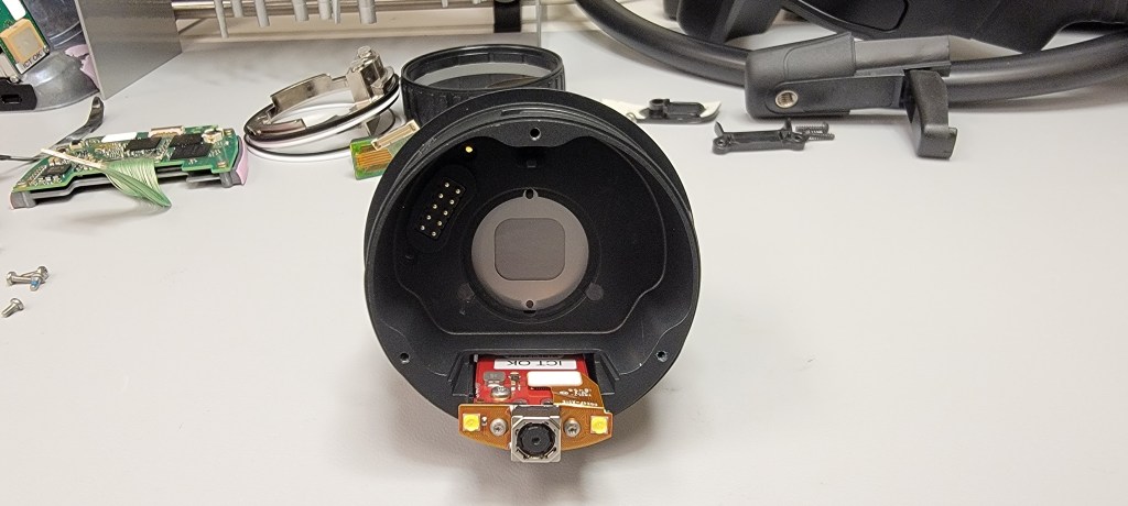
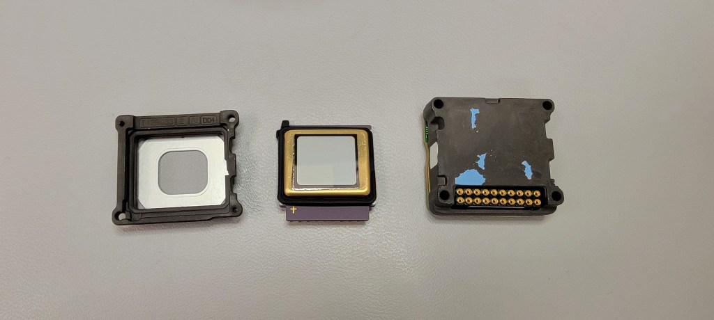
There is an interface board that connects to the lens through pogo pins. Based on this, the calibration shutter is most definitely located in the lens itself; not in the camera body where the microbolometer is.
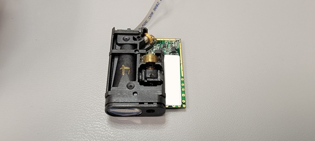
The microbolometer is mounted in a carriage that changes its distance to the static lens. This is the focal adjustment which is purely electronic. Turning the focus ring manually actually activates the motor; the direction is determined by a hall effect sensor on the ID of the focus ring barrel:
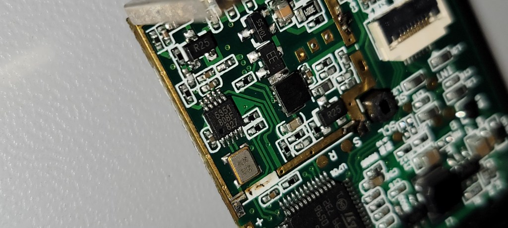
The interface board that connects to the lens:
More IC analysis:
- 18 – TI DRV8834, Dual-Bridge Stepper or DC Motor Driver
- 19 – iC Haus MHL200, 12-Bit Linear / Rotary Position Hall Encoder
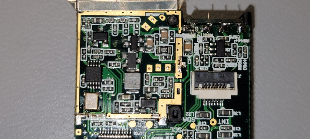
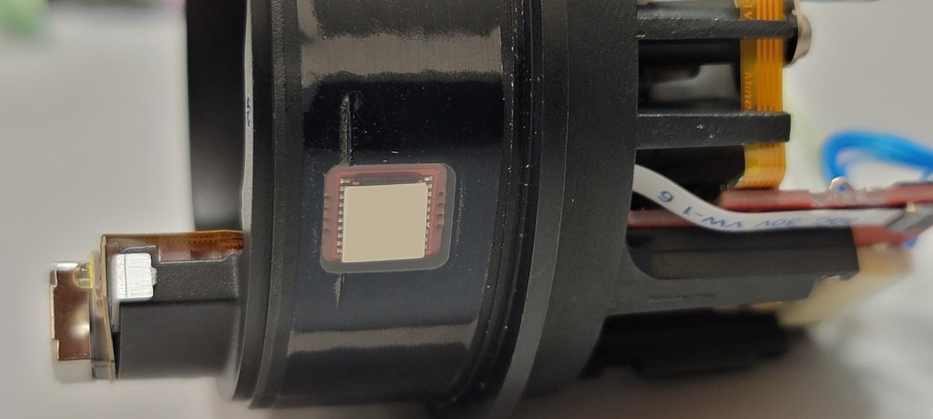
Now for the microbolometer assembly:
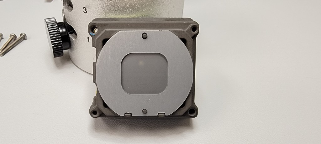
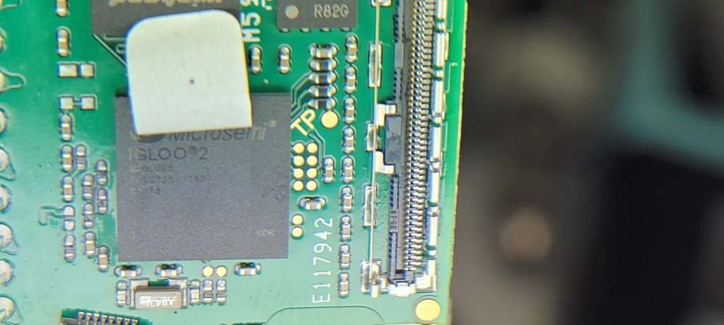
Next to the Winbond 128Mb LPDDR DRAM, we have a Microsemi Igloo 2 M2GL025 FPGA. I’m no expert on camera design, but I would imagine this local FPGA on the microbolometer board is probably some sort of high speed serial to parallel converter/preprocessor to condition sensor outputs for the DSP being done downstream in the larger Artix-7.
The sensor is sandwiched in between these metal shells to provide heatsinking. The sensor package itself appears to be ceramic.
We see another ADT7420 precision temp sensor on the microbolometer PCB, as well as a TI LM3881 power sequencer IC (the VSSOP-8 package marked STBB). There is a third National Semi marked DFN part that I can’t find any info on.
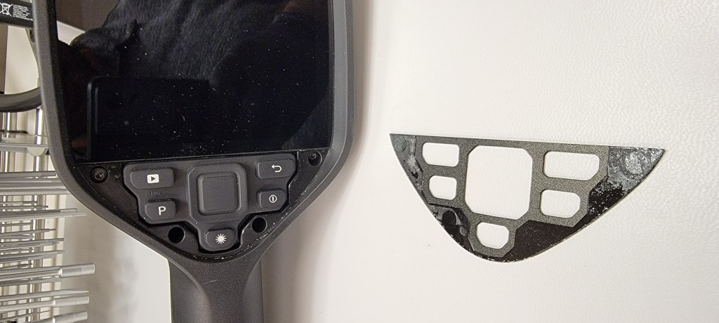
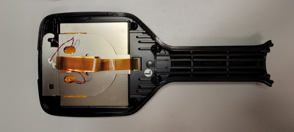
Now, moving onto the culprit behind this whole teardown, the trigger buttons for autofocus and taking pictures.
A very simple board with 2 buttons.
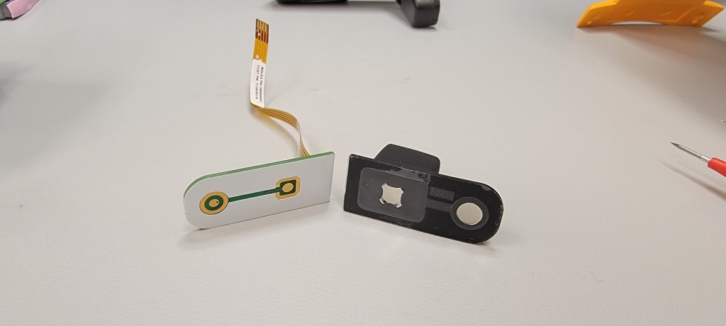
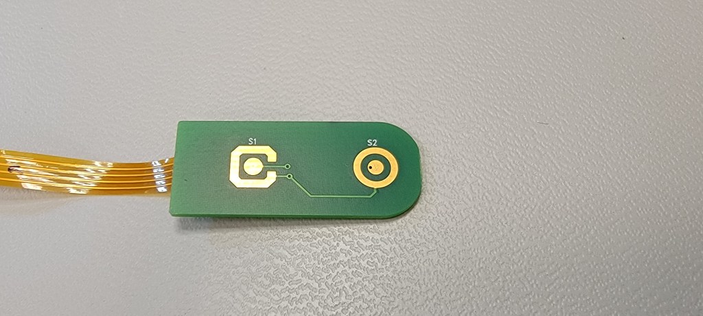
We can see that the outer ring of the switches is common, while the inner rings are what make contact. Probing the flex to the board led me to find out the issue, a cracked trace where the flex was bent 180°.
Under a microscope:
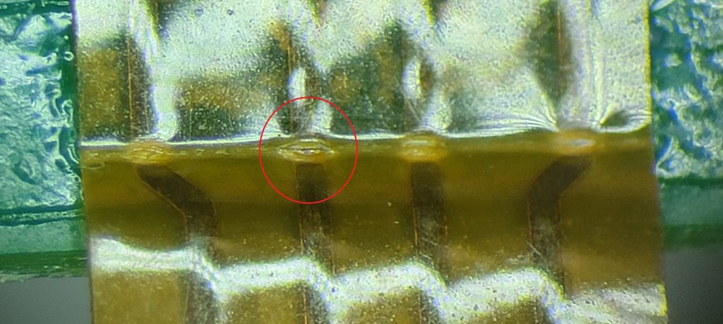
In order to repair this, I started by scraping up the flex layer to reveal more copper. I did the same treatment on all four traces (even through one was a no connect).
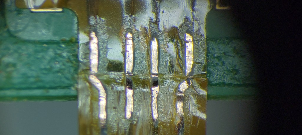
I didn’t photograph all the steps, but what I did was simple: I trimmed four small pieces of 30 gauge wire and soldered them across the flex. After cleaning, I put kapton over the exposed traces, and carefully bent them back into the original 180° position.
As a final step, I used some UV cure epoxy in a syringe to carefully irrigate around and under the radius of the bend. After curing it, the entire joint was solidly potted in the adhesive.
And that marks the end of this teardown. After a painstaking reassembly process, the camera is still working and the autofocus trigger is back to normal too!
Sort of ironic that of all the issues this complicated device could have, it was a broken trace on the simplest board! Take notes FLIR.
Until next time.
